-
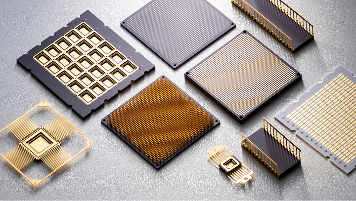
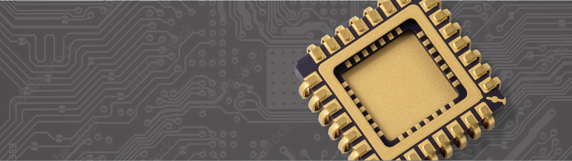
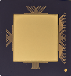
What is a Ceramic Package?
- A ceramic package is a ceramic-based housing designed to protect integrated circuits (ICs) from the external environment and ensure stable operation. With its superior heat resistance, hermeticity, and electrical insulation, it is the preferred choice for applications demanding extreme reliability.
The Roles of Ceramic Packages
-
1
Protect the IC chip from external environments (moisture, dust, light, electromagnetic waves, radiation, etc.) and temperature fluctuations.
-
2
Simplify the assembly and integration of the IC chip.
-
3
Transmit electrical signals from the IC chip without loss or degradation.
-
4
Dissipate heat generated by the IC chip to maintain stable operation.
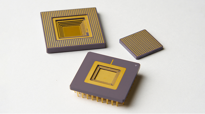
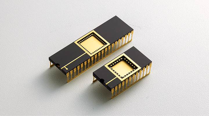
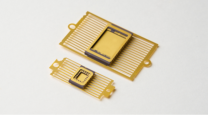
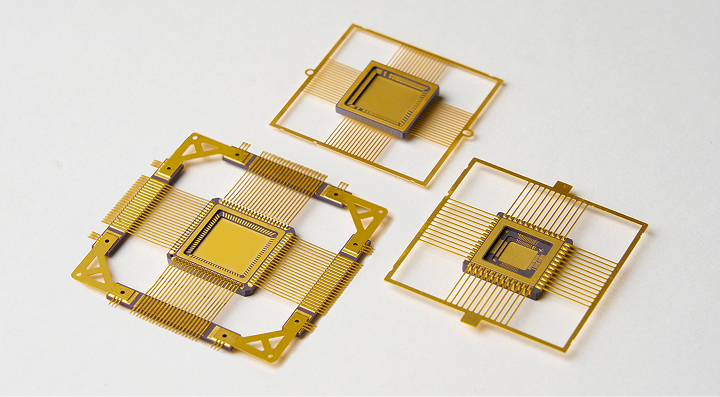
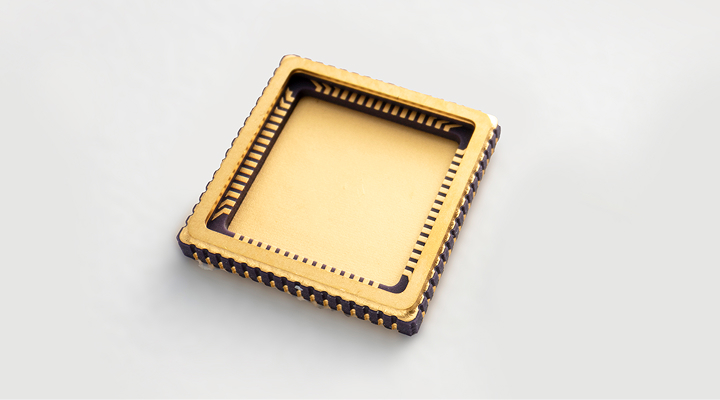
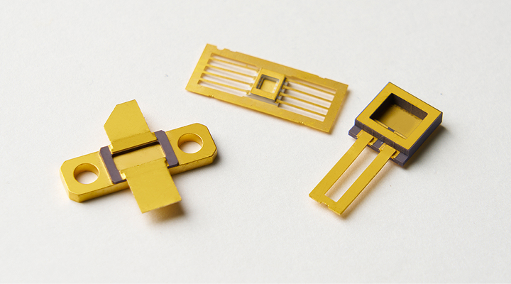
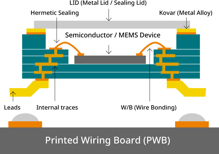
IC Chip Assembly Methods
IC chips are typically assembled into packages using either Wire Bonding or Flip Chip Bonding. After assembly, the package is hermetically sealed using a metal or ceramic lid.
-
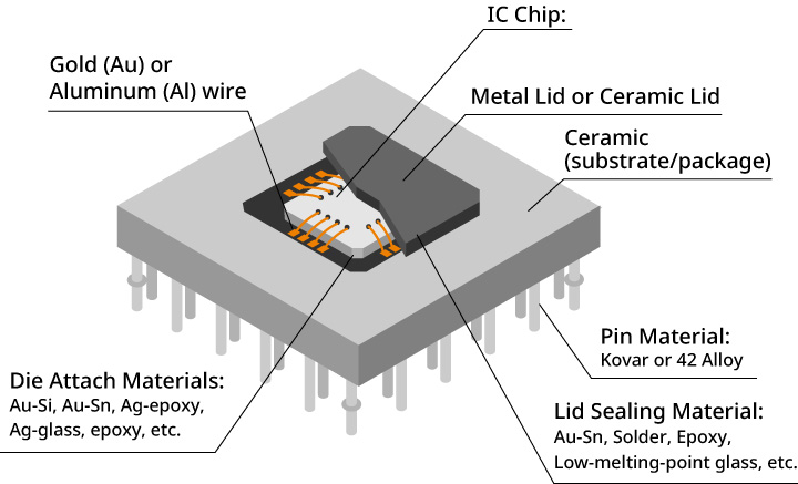
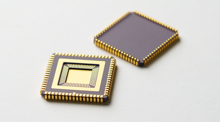
Example: Wire Bond Type
-
Wire Bonding
A method of electrically connecting the IC chip to the IC package using ultra-fine metal wires.
-
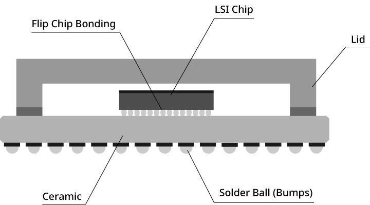
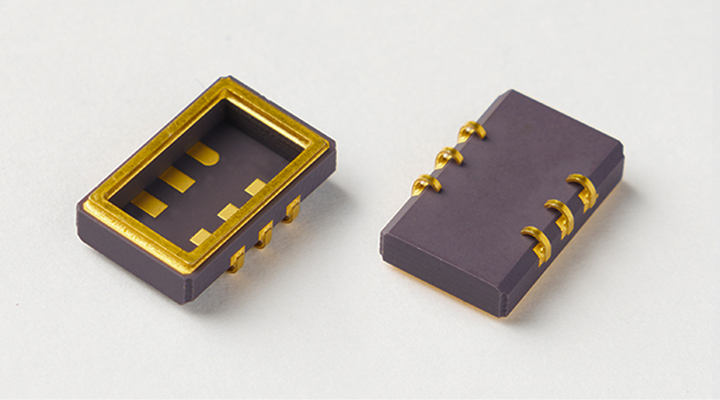
Example: Flip Chip Type
-
Flip Chip Bonding
An assembly method where the IC chip is flipped upside down and mounted directly onto the IC package via contact points (bumps).
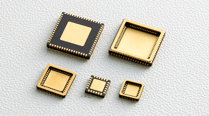
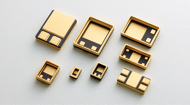
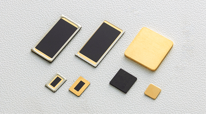
Search by Package Type
We offer a wide variety of package types to suit your mounting requirements. Please select the optimal type based on your specific application and assembly process.
Through-Hole Types (Pin Insertion)
DIP (Dual Inline Package)
SIP (Single Inline Package)
PGA (Pin Grid Array)
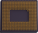
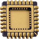
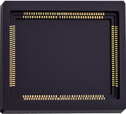
Surface Mount Technology (SMT) Types
J-Lead Type
Flat Lead Type (Gull-wing)
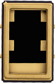
Leadless Type
BGA (Ball Grid Array)
LGA (Land Grid Array)
CSP (Chip Size Package)
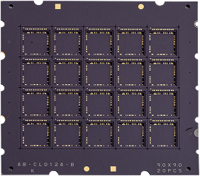
Manufacturing Process of Ceramic IC Packages
-
1
Raw Material Dispersing and Mixin

-
2
Sheet Casting

-
3
Via Punching

-
4
Via Paste Filling

-
5
Metallization / Electrode Printing

-
6
Cavity Punching

-
7
Lamination

-
8
Scoring

-
9
Co-firing

-
10
Ni (Nickel) Plating

-
11
Pre-Brazing AgCu Paste

-
12
Seal Ring metal Brazing / Attachment

-
13
Electrolytic Ni/Au Plating

-
14
Singulation by Breaking

-
15
Inspection

-
16
Shipping

Strengths and Features
-
- 01
-
Advanced Manufacturing Technology and Extensive Expertise
With decades of experience and expertise in HTCC (High Temperature Co-fired Ceramic) multilayer manufacturing, we provide tailored solutions to meet your most demanding requirements.
3D Structural Capability
From Single-layer to Multilayer Ceramics
Brazing for Various Metal Components
Versatile Plating Options (Electrolytic / Electroless)
Extensive Range of Standard Tooling
Small Lot Support
Short Lead-Time Support
-
- 02
-
Customized Design
We offer customized design proposals for ceramic package structures and layouts tailored to your specific application and requirements, even from the post-IC design phase. Please feel free to consult with us regarding your unique needs.