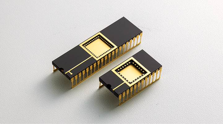
New Circuit Patterning Method
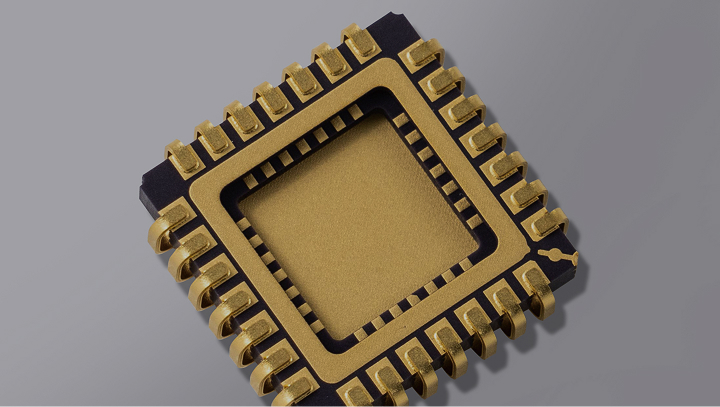
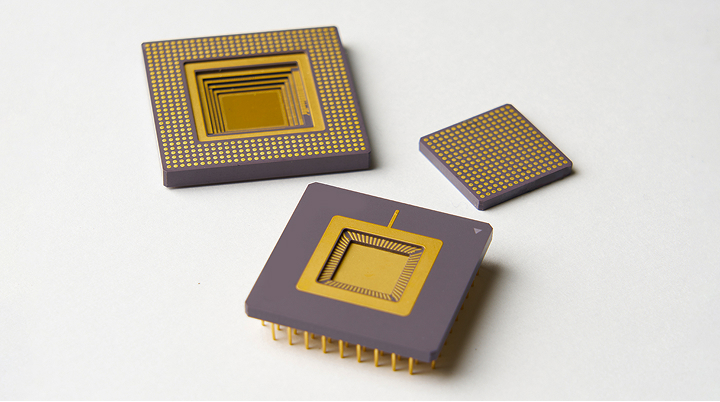
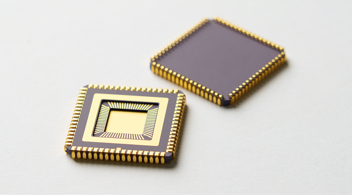
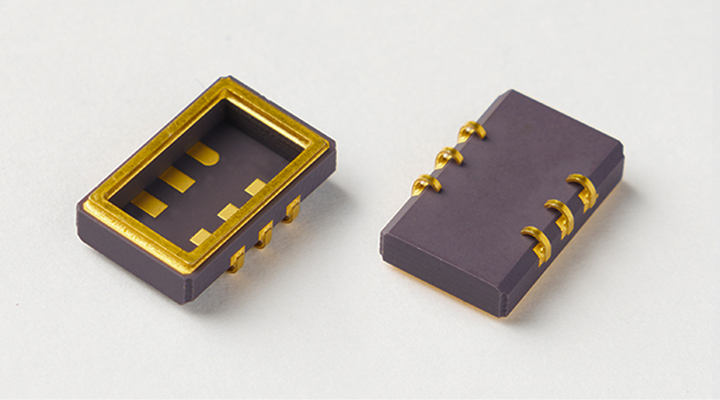
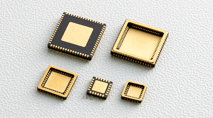
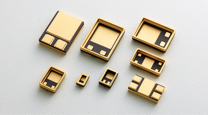
Product Concept
Advancing density and perf ormance in semiconductor packaging demand fine and high-pr ecision patterning
beyond the c apabilities of conventional printing me thods.
NTK CERAMIC developed a ne w circuit patterning method surpassing limits of conventional printing in alumina
packaging, achieving fine patterning with stable pattern shapes and high r eproducibility.
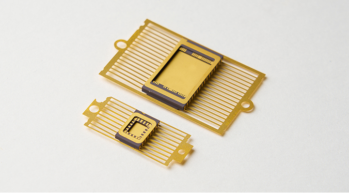
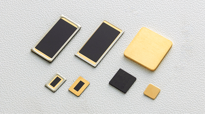
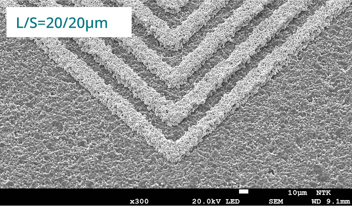
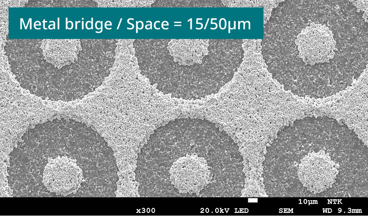
Enlarged photo
-
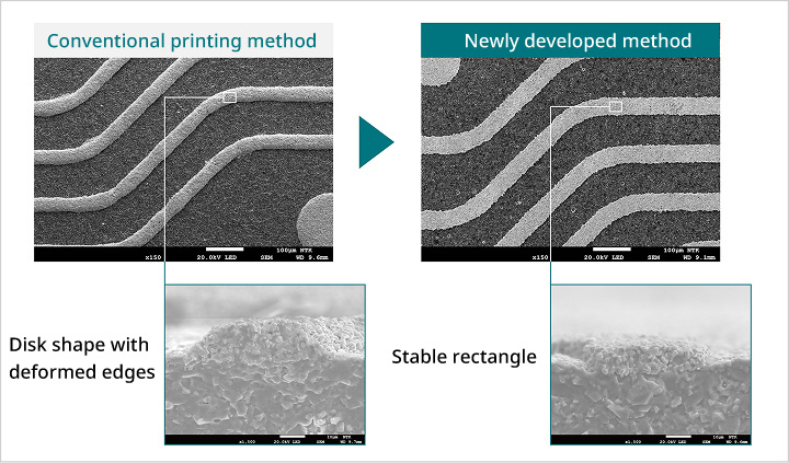
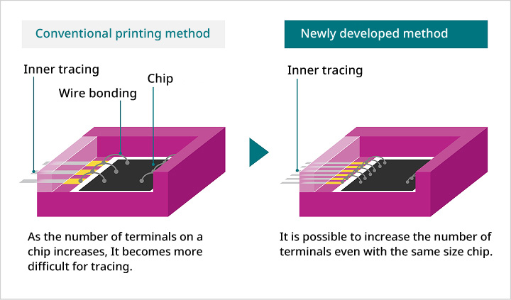
Comparison of Conventional printing method
-
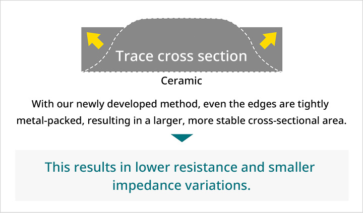
Comparison of wiring cross-sections
-
Observation at a 25 deg angle
-
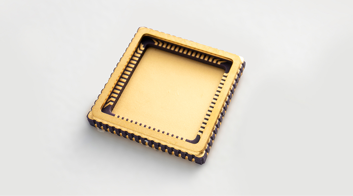
Land dia Φ50μm
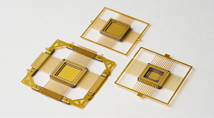
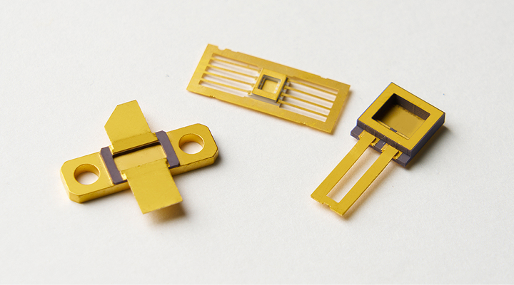
Structure
Key Features
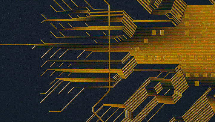
By adopting ultra-high-density wiring through our ultra-fine wiring technology, we enable our products for a wide range of applications, including high-performance semiconductor test packages and industrial packages.
- Inner signal layers L/S=20/20μm wiring
- PWR/GND layers 25μm bridge
- Sheet resistance 6mΩ□ (50μm width trace)
- Characteristic impedance 50 +/- 2Ω