View All Categories
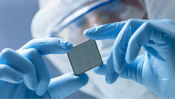
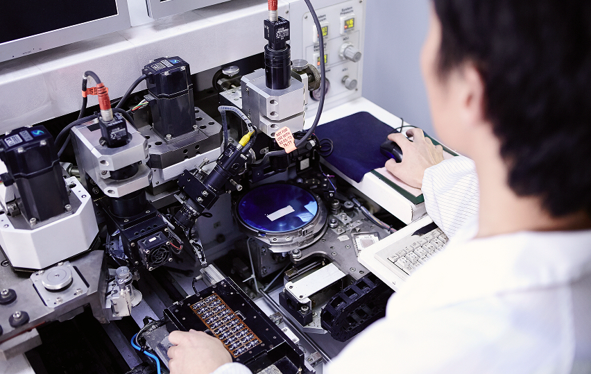
Chip Testing
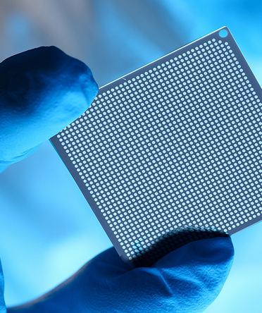
In burn-in testing, final testing, and characterization (debugging) performed after wafer testing, high-performance packages are essential to hold chips accurately and ensure stable connection with testers. NTK CERAMIC’s packages and substrates provide the specialized RF characteristics, thermal stability, and durability required to support the evaluation of advanced semiconductors with high reliability.
Our ceramic materials, featuring ultra-low dielectric constants and low dielectric loss, enable the transmission of high-speed signals in the GHz range without compromising quality – ideal for evaluating AI accelerators, CPUs, GPUs, and high-speed LSIs.
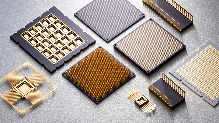
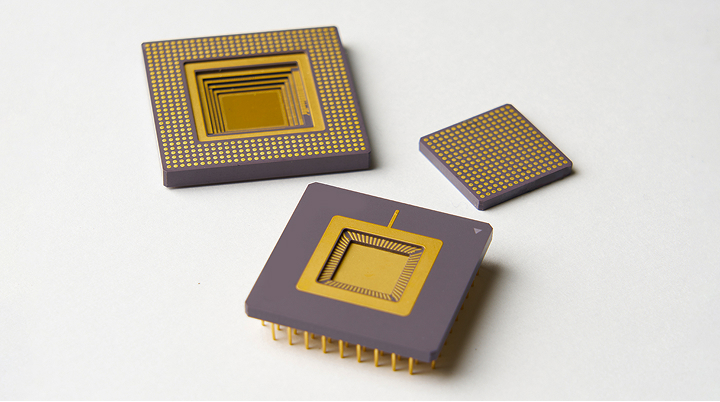
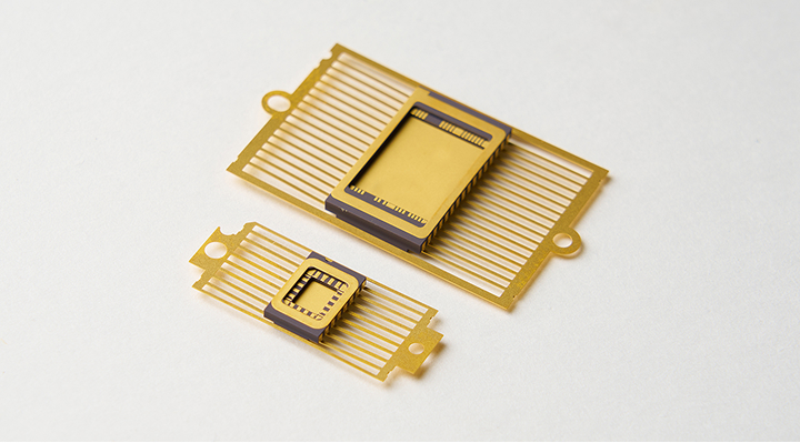
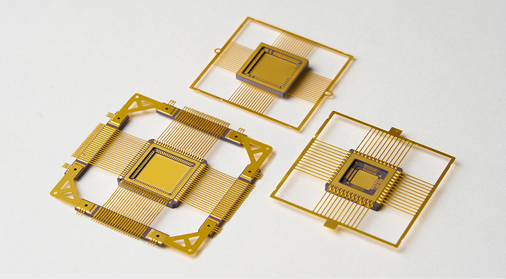
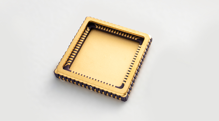
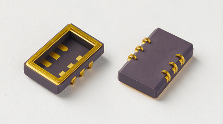
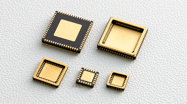
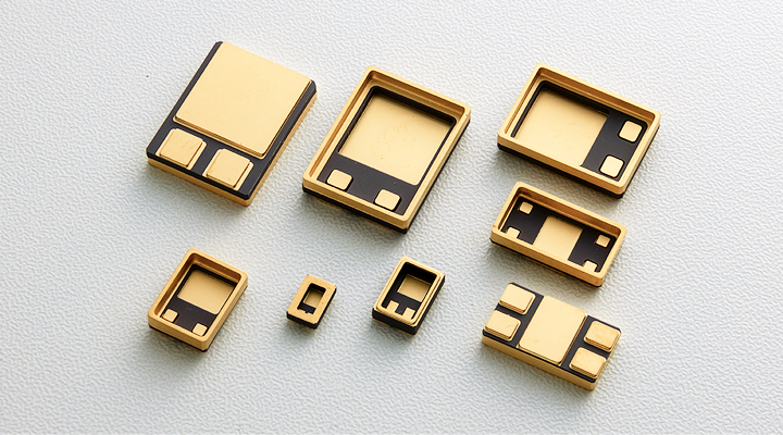
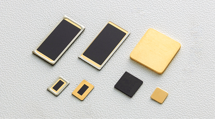
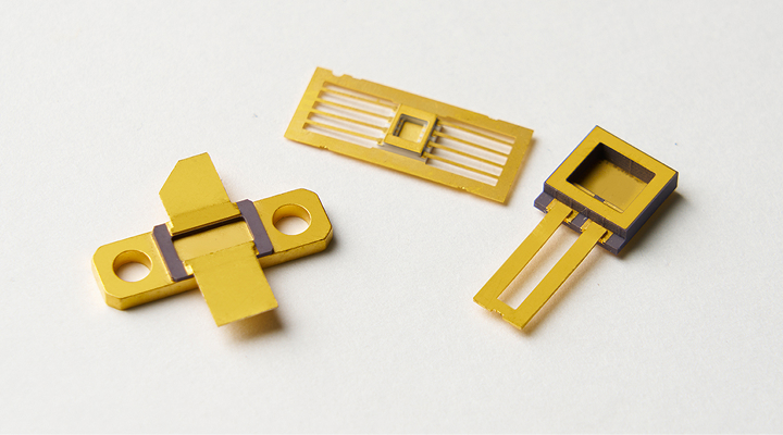
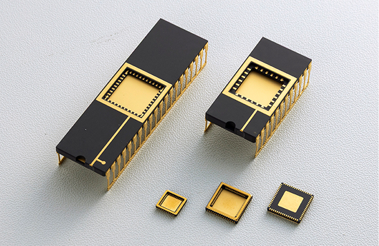
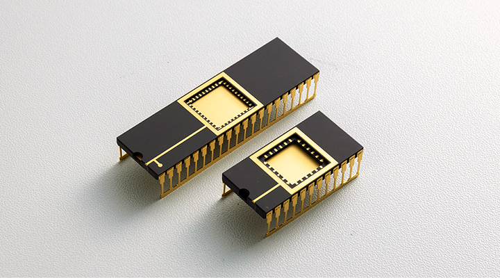
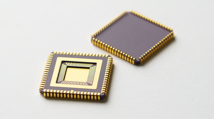
Package Lineup
- Applications and Key Fields
-
In the chip testing process, the package must provide a high-precision and highly reproducible environment, as it directly impacts device quality and yield. With the increasing complexity of semiconductors for AI, high-speed communications, and data centers, test substrates now require advanced RF compatibility, high-density wiring, and superior thermal management.
NTK CERAMIC provides the high-reliability packages needed to meet these rigorous demands, supporting the high-precision evaluation of advanced chips over the long term.Key Applications
- Chip Testing
Product Features and Strengths
-
- 1. Ultra-Low Loss and High Reproducibility
- In testing GHz-range semiconductors, transmitting high-speed signals without degradation is essential. Our ceramic packages feature ultra-low dielectric constants and loss tangents, minimizing signal loss, reflection, and crosstalk. This ensures high-level reproducibility and measurement accuracy even for high-speed AI chips and processors, contributing to improved debugging efficiency and shorter evaluation times.
-
- 2. Thermal Stability for High-Temperature Testing
- Burn-in tests require devices to operate at high temperatures for extended periods. Our packages combine high thermal conductivity to suppress temperature drift with a low CTE to reduce stress. With durability that withstands heat over 125°C, they maintain stable measurement conditions and resist deformation during repeated thermal cycling, offering a long-life solution for testing processes.
-
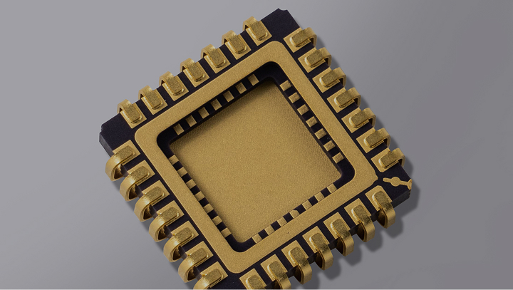
- 3. Precision and High-Density Multilayer Technology
- Test sockets must ensure reliable contact for thousands of terminals with micron-level precision. The high rigidity of ceramics prevents misalignment and deformation under repeated mechanical loads and heat. Furthermore, our HTCC technologies enable high-density multilayer wiring, high thermal resistance and high thermal dissipation allowing complex evaluation environments to be optimized within the package itself.
- Initiatives for the Next Generation
- As semiconductor devices become faster and more powerful, chip test packages must offer even higher frequency compatibility, thermal management, and precision. NTK CERAMIC is actively driving the development of next-generation test environments through low-dielectric materials, high-thermal-conductivity ceramics, advanced multilayer wiring, and ceramic-metal hybrid structures.
By enhancing measurement accuracy, evaluation reproducibility, and reliability for AI, data centers, automotive, and telecommunications, we continue to evolve our foundational technologies to ensure the quality of future semiconductors.

-
Consultation &
Customized Design -
Proposing optimal ceramic package structures and designs tailored to your needs.
"Complex geometries?" "Strict specs?" "Beyond rules?"
We respond flexibly to every unique challenge to co-create your optimal solution.
Please feel free to contact us.