View All Categories
Imaging Devices
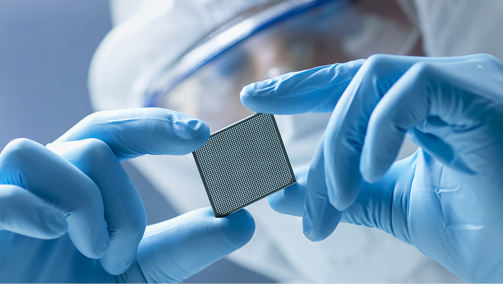
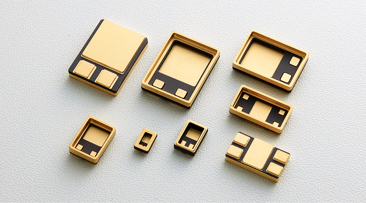
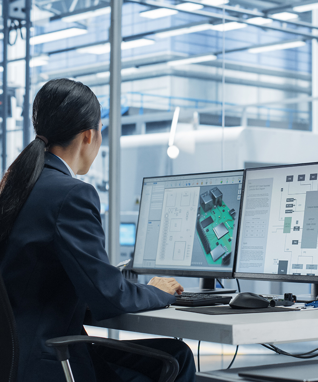
Imaging devices serve as the essential “eyes” of modern technology, converting light into electrical signals across a wide range of applications – from smartphones and digital cameras to surveillance, automotive cameras, medical endoscopes, and aerospace equipment.
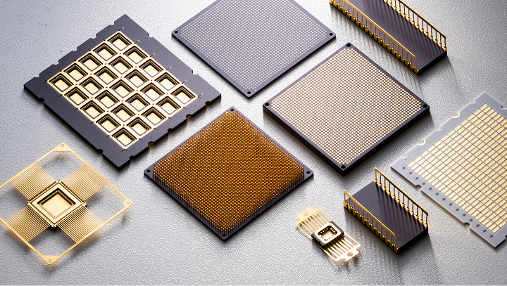
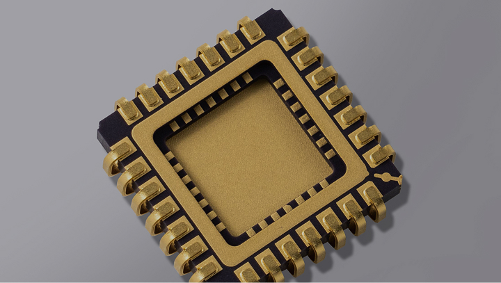
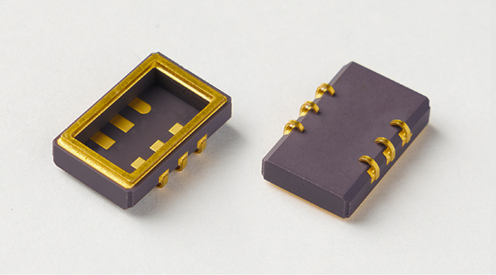
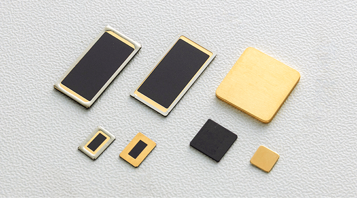
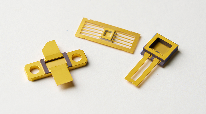
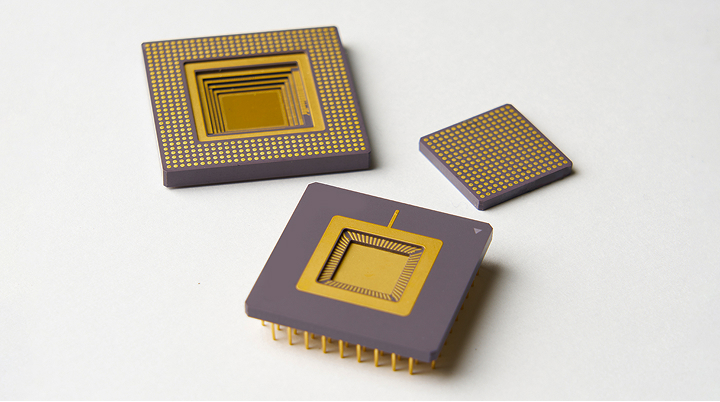
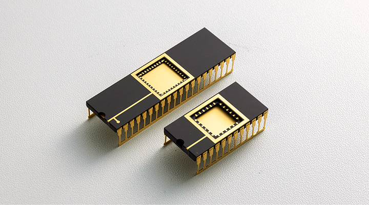
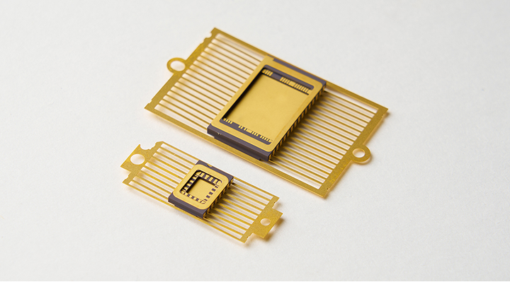
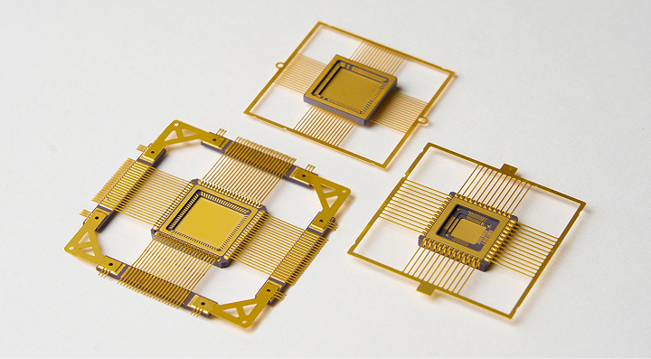
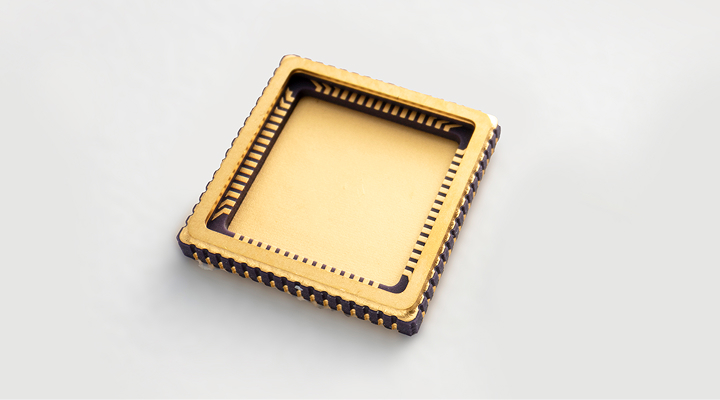
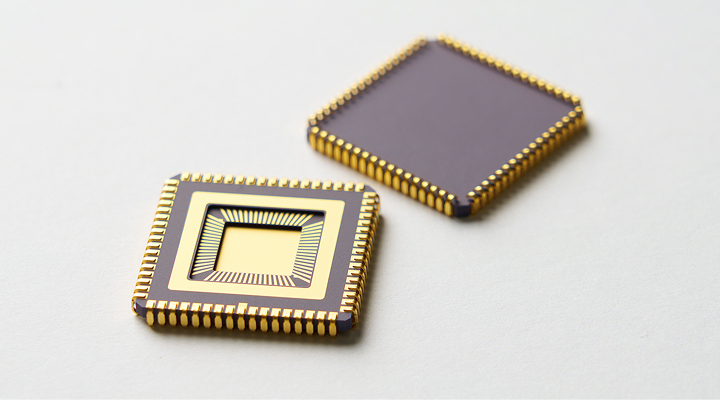
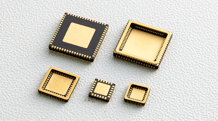
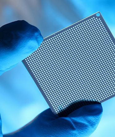
Because imaging sensors (CMOS/CCD) are highly sensitive to light, they are extremely delicate and vulnerable to impurities or environmental changes. NTK CERAMIC’s packages serve as the vital foundation for these sensor chips, protecting them while maximizing their performance potential.
- Applications and Key Fields
-
Imaging devices are used in a vast range of sectors, from everyday consumer electronics to ultra-high-precision industrial and aerospace applications. In the consumer and mobile markets, smartphone image sensors are the most prominent example.
In the industrial and factory automation sectors, these devices are essential for sorting and inspection scanners, large-scale linear sensors, surveillance cameras, and baggage screening systems. In the medical field, they play a critical role in X-ray imaging systems.
Product Features and Strengths
-
- 1. Superior Flatness and Rigidity
- Even slight distortions in an image sensor chip can lead to poor focus and blurred edges, a problem that becomes more pronounced as sensor sizes increase. Ceramics offer significantly higher rigidity than resin materials, enabling micron-level flatness that remains stable over time. This high rigidity minimizes warping caused by thermal stress, ensuring exceptional resolution and clarity across the entire image.
-
- 2. Advanced Thermal Management
- High-resolution, high-speed image sensors generate heat that increases "dark noise," leading to significant image degradation. Using high-thermal-conductivity ceramics, such as Alumina and Aluminum Nitride, our packages efficiently dissipate heat away from the chip. By suppressing thermal noise, we ensure consistent image quality during continuous operation - a critical advantage for surveillance and automotive cameras.
-
- 3. High Reliability
- For imaging devices used in the aerospace sector, where systems are exposed to extreme environments, the superior stability and durability of our ceramic packages provide an essential competitive edge.
- Initiatives for the Next Generation
- As imaging devices grow in size and complexity, we are refining higher flatness, superior heat dissipation, and finer wiring.
We are also developing ceramics with even greater dimensional stability to support the integration of multiple sensors into a single package. Our goal is to provide the reliable foundation needed for the next generation of high-performance imaging.
-
Consultation &
Customized Design -
Proposing optimal ceramic package structures and designs tailored to your needs.
"Complex geometries?" "Strict specs?" "Beyond rules?"
We respond flexibly to every unique challenge to co-create your optimal solution.
Please feel free to contact us.