View All Categories
MEMS Devices
MEMS (Micro Electro Mechanical Systems) devices are used in a wide range of applications, including physical sensors for pressure, acceleration, and gyroscopes, as well as micromirrors for optical switches and microactuators for DNA testing.
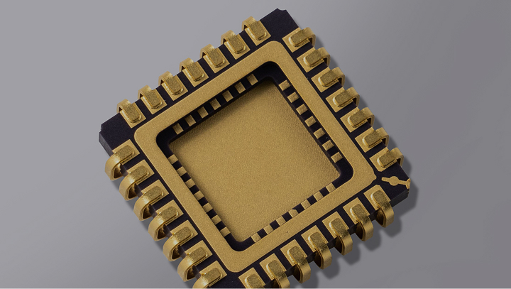
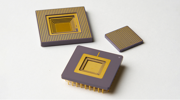
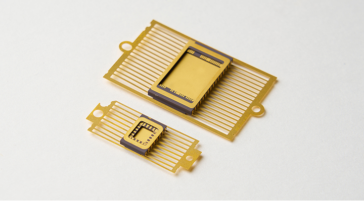
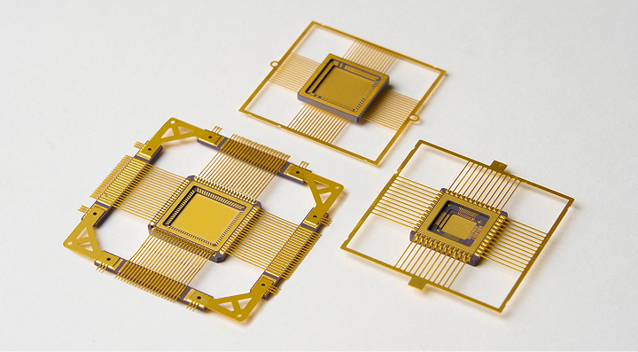
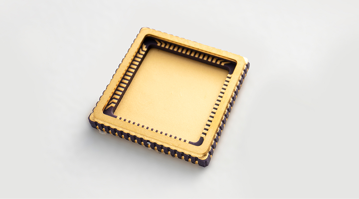
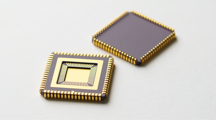
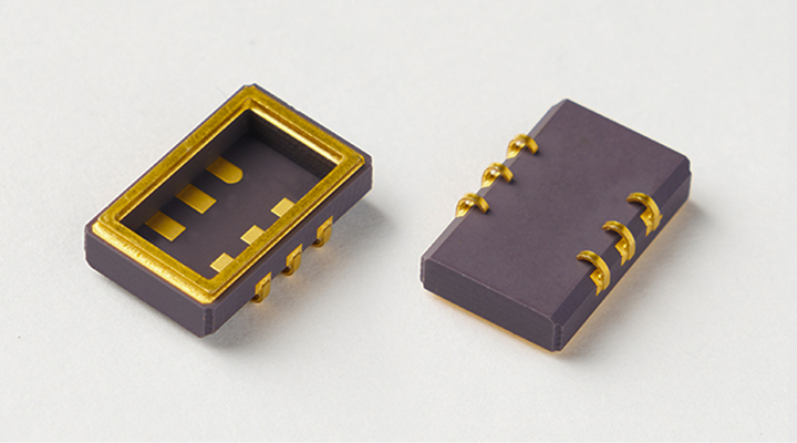
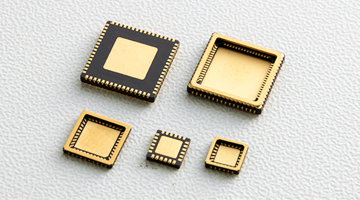
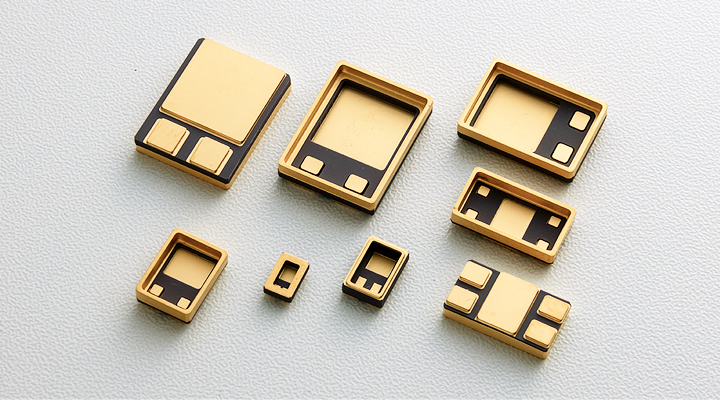
NTK CERAMIC’s packages function as compact, highly reliable multilayer wiring substrates that significantly contribute to the overall reliability of these devices. In the aerospace industry, where MEMS devices face the most stringent requirements, our ceramic packages provide the uncompromising performance needed to meet those demands.

- Applications and Key Fields
-
In Aerospace, our packages are used for inertial sensors like gyroscopes in satellites and rockets. Their radiation resistance and high hermeticity ensure stable operation and precise attitude control in the vacuum of space.
In Information and Communications, our products support the next generation of data centers by housing optical switches that dynamically connect large-scale AI clusters.
In Industrial and Factory Automation, ceramic packages protect micromirrors in maskless lithography systems and specialized sensors for oil drilling that must withstand extreme pressure, heat, and magnetism.
In Medical and Environmental fields, our technology provides the stability required for high-precision DNA sequencers and ensures the durability of airflow, water quality, and wind power sensors.
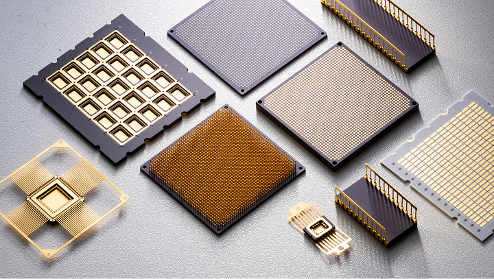
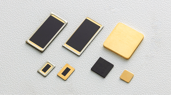
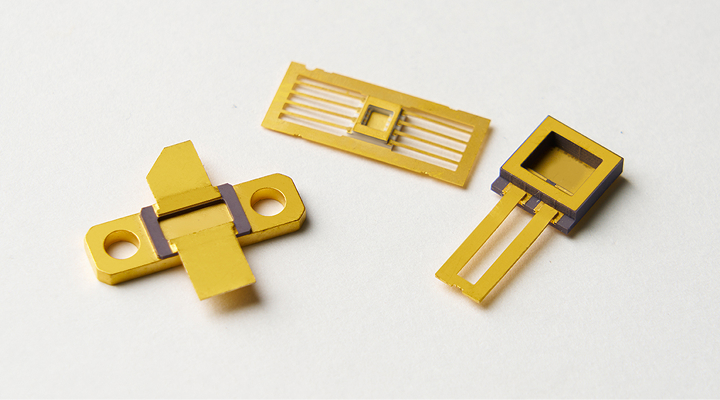
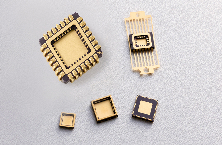
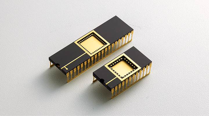
Product Features and Strengths
-
- 1. Hermeticity and Environmental Resistance
- MEMS devices feature delicate moving parts that require protection from physical contact and atmospheric degradation. Our ceramic packages provide essential high hermeticity to ensure long-term stability. In aerospace, they minimize failure risks under intense radiation, while for oil drilling, they withstand extreme pressure and heat. We also offer non-magnetic metallization to ensure precision in magnetic field sensing.
-
- 2. Mechanical Stability for Peak Performance
- To maintain the high precision of MEMS operations, the packaging must not deform. Our ceramics offer superior flatness, high rigidity, and low thermal expansion, ensuring that the device's internal structures remain perfectly aligned under all conditions.
-
- 3. Flexible Customization
- With a fully integrated in-house manufacturing process, we provide flexible support and custom designs tailored to the unique specifications of diverse MEMS devices.
- Initiatives for the Next Generation
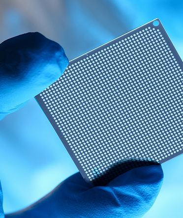
- To meet the demands of next-gen MEMS, we are advancing core technologies for high heat dissipation, low resistance, and fine-line ceramic packaging.
To achieve high-density multilayering, we are developing high-definition patterning and Low electrical resistance, High-strength substrate for lower-resistance wiring. We are also enhancing high flatness and low-warpage solutions for larger devices like optical switches.
Since MEMS possess intricate mechanical structures, our ceramic packages act as "protective suits" against harsh environments, a "stable foundation," and a "framework" that maximizes device performance and reliability.

-
Consultation &
Customized Design -
Proposing optimal ceramic package structures and designs tailored to your needs.
"Complex geometries?" "Strict specs?" "Beyond rules?"
We respond flexibly to every unique challenge to co-create your optimal solution.
Please feel free to contact us.