View All Categories
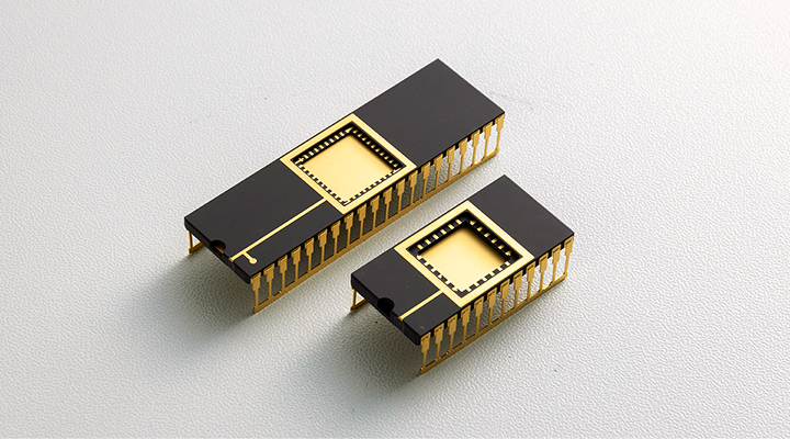
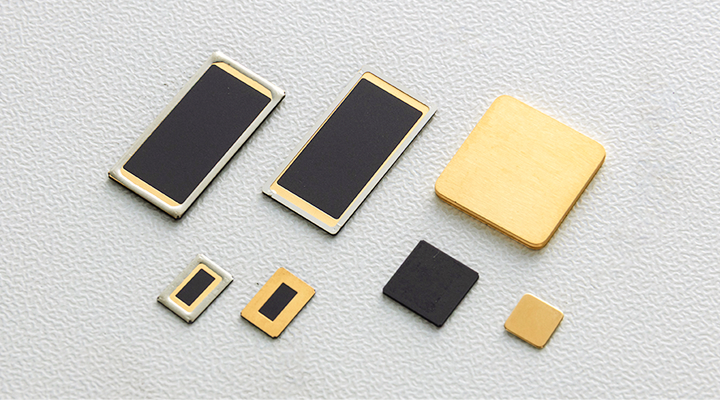
Probe Cards
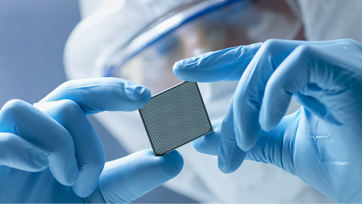
A probe card is a critical interface that electrically connects the semiconductor chips on a wafer to a tester during the wafer-level electrical testing process (front-end of line).
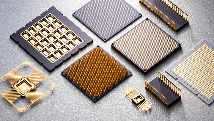
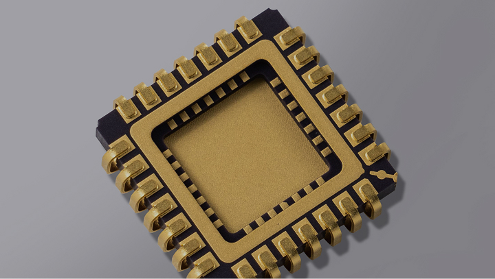
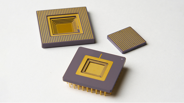
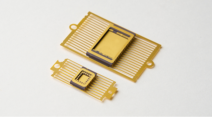
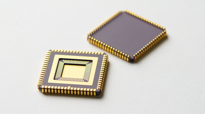
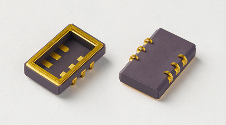
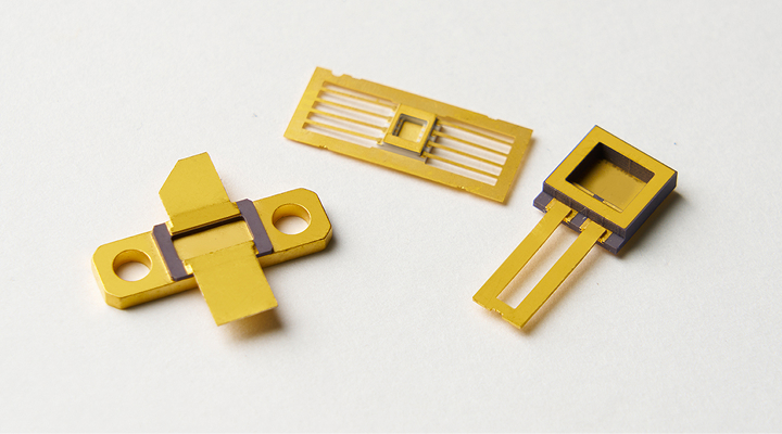
The card features microscopic probes that make contact with the chip electrodes on the wafer, delivering electrical signals from the tester to the chip with zero degradation.The backbone of this probe card is the STF (Space Transformer), which is crafted from NTK CERAMIC’s high-performance ceramic materials.
As a relay substrate, the STF supports the precise alignment of the probes and ensures stable signal transmission – playing a fundamental role in maintaining the highest inspection quality.

- Applications and Key Fields
-
Driven by recent advancements in AI technology, data centers are processing massive amounts of calculations and data. The processors and memory chips supporting these operations are becoming faster, more powerful, denser, and larger, all while demanding lower power consumption. Consequently, inspection technologies must achieve ever-higher levels of precision.
Furthermore, as the speed of semiconductor development accelerates, we are required to respond with agility - completing probe cards within just a few months of the initial chip design.Key Applications
- Logic Devices
- Memory (HBM: High Bandwidth Memory)
Product Features and Strengths
-
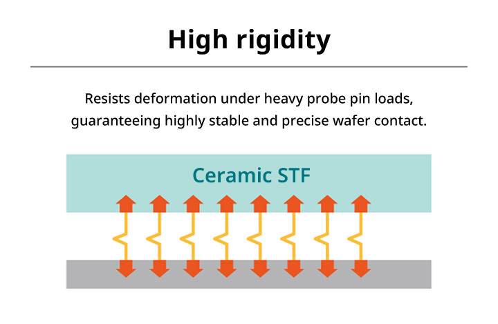
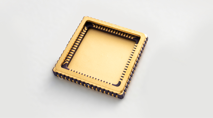
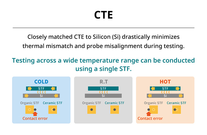
- 1. High-Precision Inspection via High Rigidity and Superior Flatness
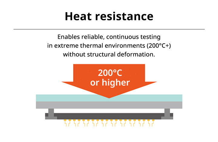
- Our STF (Space Transformer) combines high rigidity and a low Coefficient of Thermal Expansion (CTE) with excellent heat resistance and high flatness. By minimizing deformation caused by temperature fluctuations or external forces, it maintains stable probe pitch and planarity.
This ensures that even as semiconductor wafers increase in size, each probe makes reliable contact with the electrodes, enabling high-quality inspection.
-
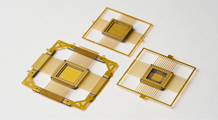
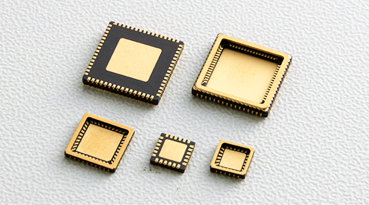
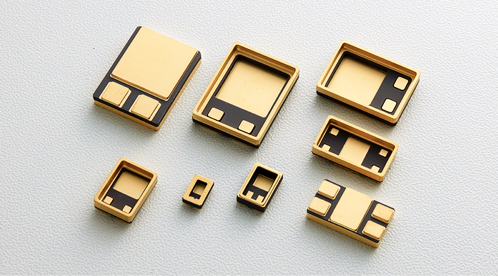
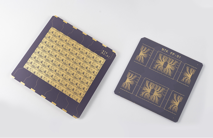
- 2. Large-Scale, Multilayer, and High-Density Structures
- We have achieved a multilayer structure of up to 50 layers with a maximum size of 170mm square.
Our high-density wiring technology supports the inspection of large-area wafers for logic and memory devices.
As semiconductors continue to grow in size and integration, our products support stable electrical characteristics and high-precision signal transmission.
-
- 3. Balancing Customization with Short Lead Times
- Our integrated production system with dedicated lines enables the fastest possible delivery for custom orders.
- Initiatives for the Next Generation
- We are currently developing a hybrid structure of ceramics and resin to improve electrical characteristics and achieve finer circuit patterns.
We continue to aim to realize high-performance STFs that meet the rigorous demands of next-generation semiconductor testing.
-
Consultation &
Customized Design -
Proposing optimal ceramic package structures and designs tailored to your needs.
"Complex geometries?" "Strict specs?" "Beyond rules?"
We respond flexibly to every unique challenge to co-create your optimal solution.
Please feel free to contact us.